Condensed Matter Experiment Ⅰ
Functional Properties of Thin Film Interface
Staff
| Professor : | Masao Nakamura |
Research
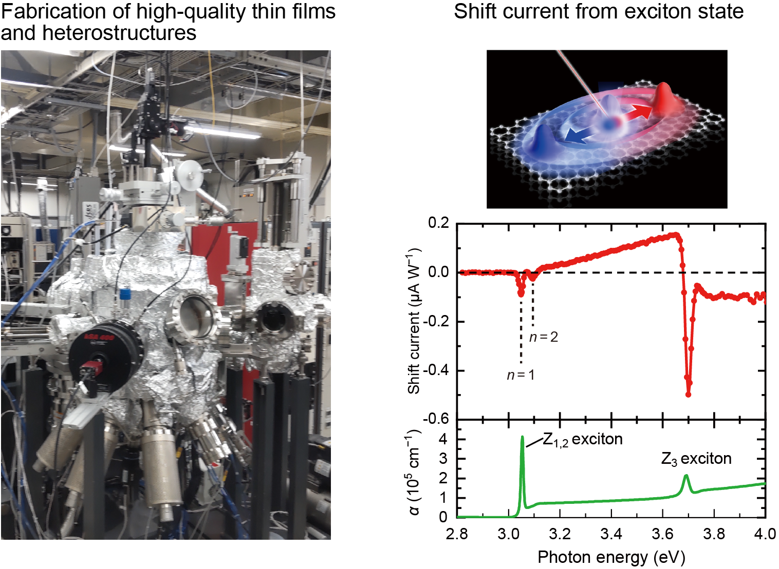
Heterointerfaces exhibit electronic states distinct from those of the individual constituent materials due to the changes in dimensionality, charge transfer at the interface, and proximity effects. We investigate the physical properties of thin films and heterostructures composed of strongly correlated electron systems, where electrons interact intensely with each other, and topological materials, where the geometric phases of electrons govern macroscopic properties. By employing molecular beam epitaxy (MBE) and pulsed laser deposition (PLD) techniques, we fabricate high-quality thin films and heterostructures to explore novel quantum phenomena and functionalities emerging at their interfaces.
The following topics are currently under investigation.
- Experimental demonstration of nontrivial characteristics of shift current that arising from quantum geometric properties, while also exploring materials capable of generating shift current with higher efficiency
- Epitaxial growth of halide perovskite thin films by molecular beam epitaxy to explore their potential for enhancing photovoltaic performance to reveal new aspects of halide perovskite as quantum materials
- Electric-field and optical control of electronic phases at designed heterointerfaces of strongly correlated electron materials
- Exploration of emergent phenomena in thin films and superstructures of quamtum materials induced by the symmetry breaking and magnetic proximity effect at heterointerfaces