Condensed Matter Experiment II
Quantum Dynamics
Laboratory Website:
http://quantum.phys.tohoku.ac.jp/
Academic Staff
- Professor/Go Yusa
- Assistant Professor/Katsushi Hashimoto
- Assistant Professor/Nicholas Moore
About Research
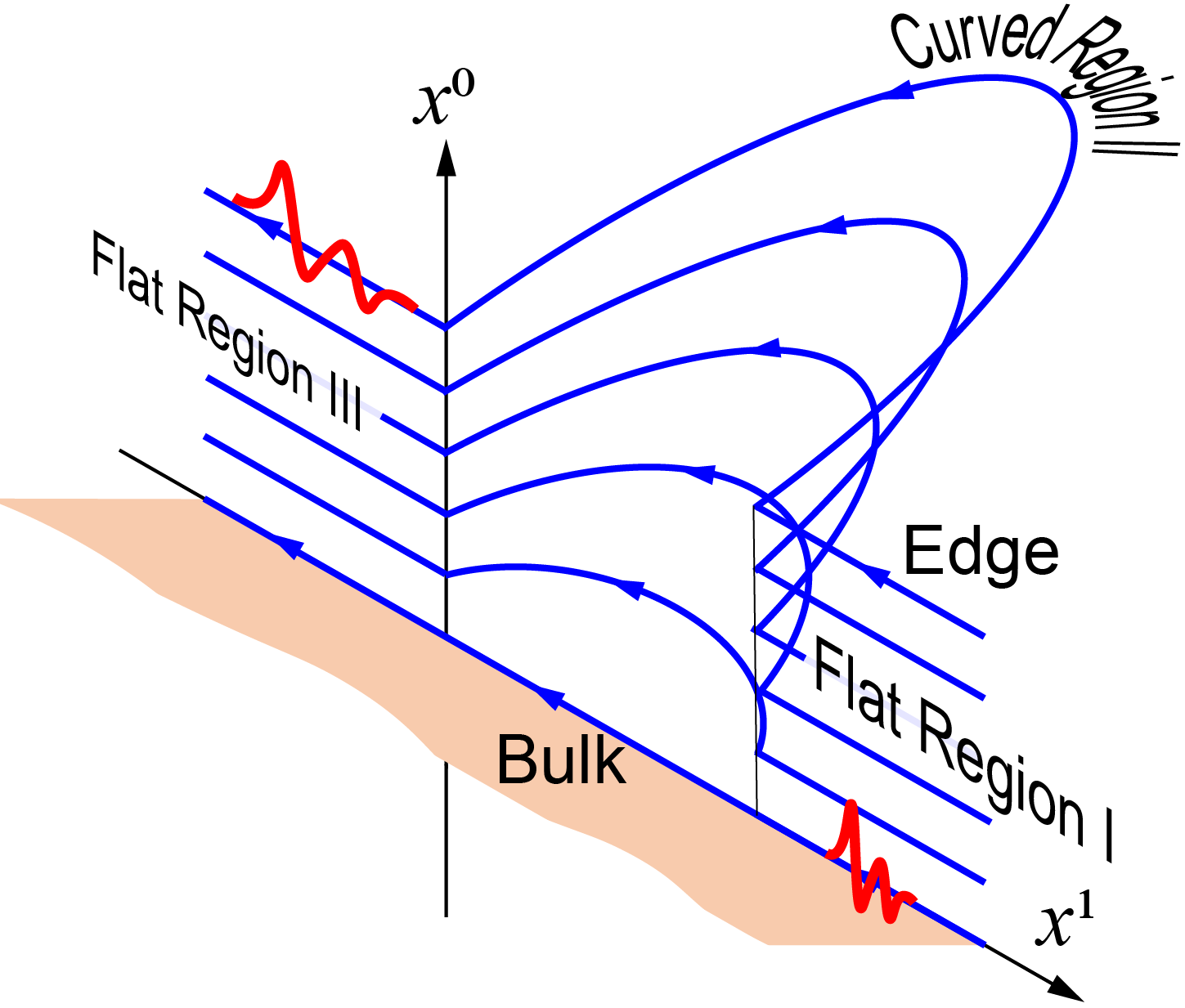
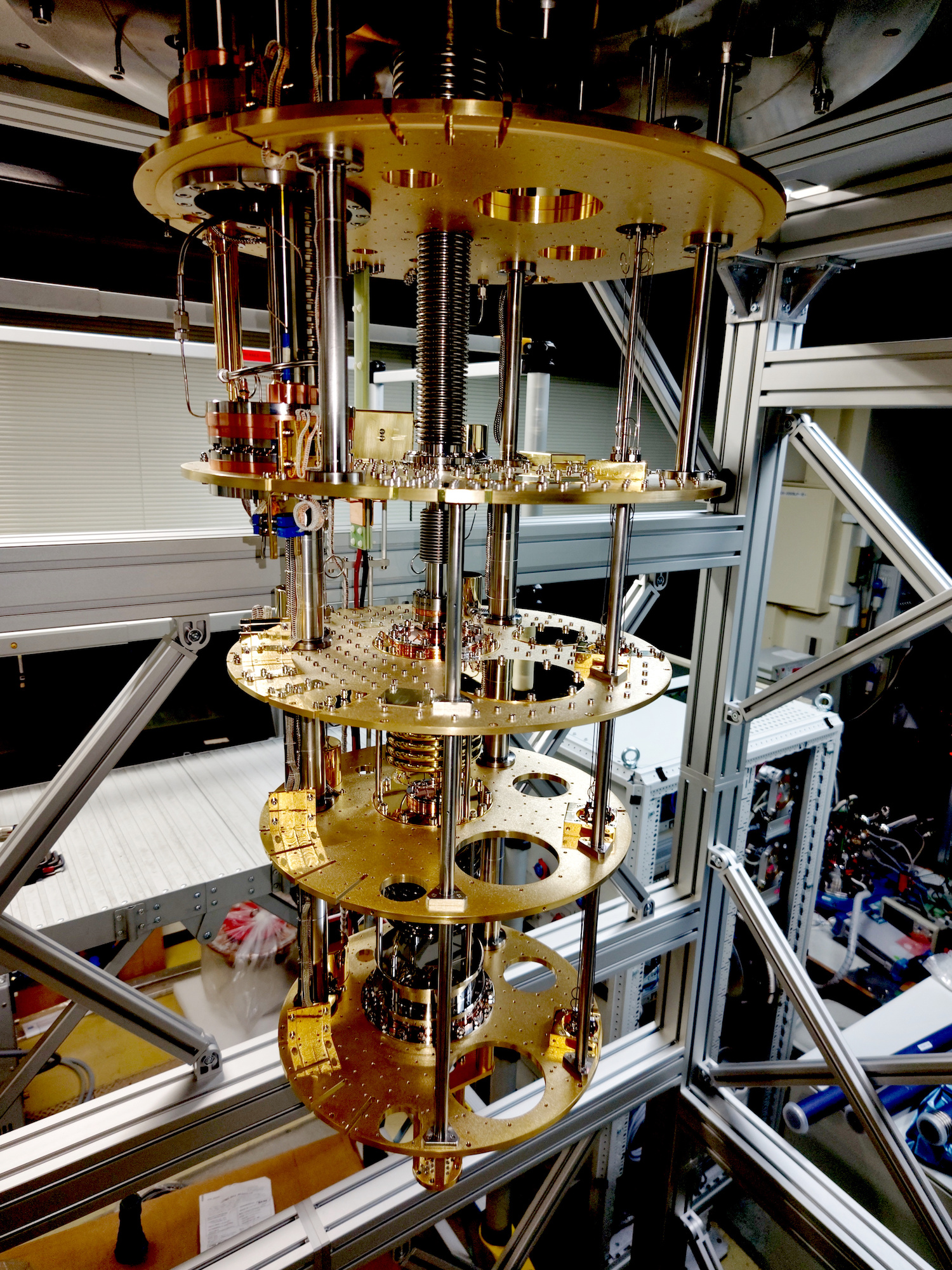
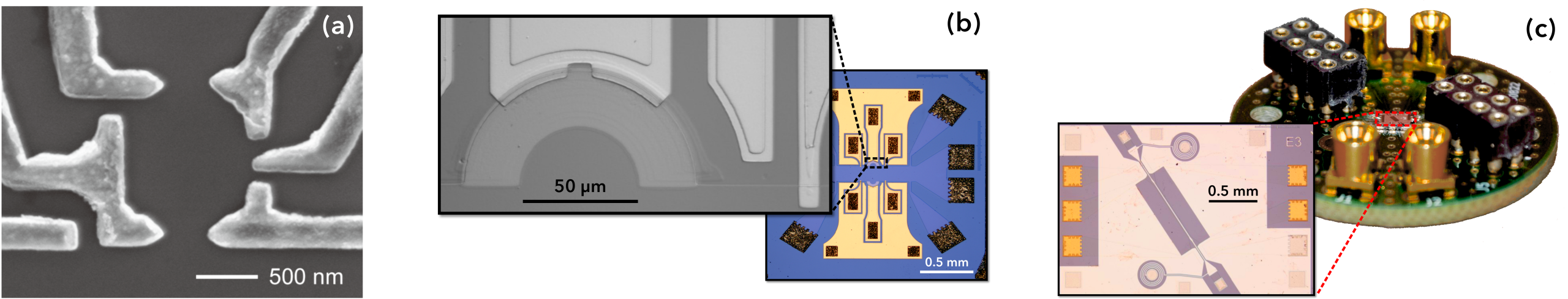
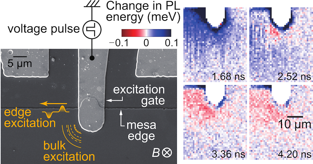
The semiconductor industry which underpins our daily lives within modern society consists of a broad range of advanced technologies, including ultra-high-quality crystal growth, device fabrication, high-frequency measurement techniques, and optical technologies. Building on these advanced technologies and using ultra-high-purity semiconductor devices and novel materials, we seek to realize toy models—simplified physical models that extract and test essential physics—for investigating diverse spacetime phenomena, including the “quantum universe” that emerges in black holes, wormholes, the Big Bang and in the early stages of cosmic creation. Towards this goal we dynamically control a variety of quantum degrees of freedom and their collective excitations, such as electrons, holes, excitons, nuclear spins, and plasmons, within nanostructures realized in low-dimensional semiconductor systems where striking manifestations quantum mechanics occur. Using electrical and optical measurements—especially time-resolved measurements—as a foundation, we approach the system dynamics from the complementary perspectives of electronics and photonics. This kind of research is expected to extend beyond the astronomical and astrophysical motivations of understanding the universe we inhabit, and to develop into an experimental inquiry into more universal physical laws and dynamical principles.